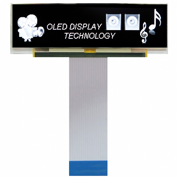

 WG25664A1W
|
Item |
Description |
|
Product No. |
WG25664A1WITF000 |
|
Active Area |
76.78(W)mm×19.18(H)mm |
|
Viewing Area |
78.78(W)mm×21.18(H)mm |
|
Module Size |
88.00(W)×27.80(H)×6max(D) |
|
Dot Size |
0.28(W)mm×0.28(H)mm |
|
Dot Pitch |
0.3(W)mm×0.3(H)mm |
|
Display Format |
256(W)×64(H) Dots |
|
Duty Ratio |
1/64 Duty |
|
Controller |
SSD1322 |
詳細資料 Description

INTERFACE PIN ASSIGNMENT
|
No. |
Symbol |
Function |
|
1 |
VDD |
Power supply for analog circuit. |
|
2 |
VSS |
Ground. |
|
3 |
Vo |
Contrast Adjustment |
|
4~11 |
D0~D7 |
Data bus. |
|
12 |
CS# |
Chip select input. |
|
13 |
NC |
No connection |
|
14 |
RES# |
Reset signal input. When it’s low, initialization of SSD1309 is executed. |
|
15 |
R/W# |
Data write operation is initiated when it’s pull low. |
|
16 |
D/C# |
Data/ Command control. Pull high for write/read display data. Pull low for write command or read status. |
|
17 |
E/RD# |
Data read operation is initiated when it’s pull low. |
|
18 |
NC |
No connection |
|
19 |
DISP |
Display off |
|
20 |
NC |
No connection |
ELECTRICAL CHARACTERISTICS
|
Item |
Symbol |
Condition |
Min. |
Typ |
Max. |
Unit |
|
Power Supply for Logic |
VDD |
(Wide Voltage I/O Application) |
2.7 |
3 |
3.5 |
Volt |
|
Input Voltage for I/O Pins |
Vi |
2.7 |
3 |
3.5 |
Volt |
|
|
Input Voltage |
VIL |
L level |
0 |
- |
0.2 VDD |
Volt |
|
VIH |
H level |
0.8 VDD |
- |
VDD |
Volt |
|
|
Output Voltage |
VOL |
L level |
0 |
- |
0.1 VDD |
|
|
VOH |
H level |
0.9 VDD |
- |
VDD |
|
|
|
Power Supply Current for OLED |
IDD |
Note |
- |
100 |
|
mA |
|
Sleep Mode Current for VDD |
IDD,SLEEP |
|
|
2 |
10 |
μA |
Note : VDD = 3.0V, 50% Display Area Turn on.80 cd/m2
When random texts pattern is running , averagely , about 1/2 of pixels will be on.


